Introduction
OrCAD is a powerful software suite used for electronic design automation (EDA), enabling students and professionals to design, simulate, and analyze electronic circuits. It is an essential tool in electrical and electronics engineering, providing solutions for PCB (Printed Circuit Board) design, schematic capture, and simulation. However, mastering OrCAD can be challenging, leading many students to seek OrCAD Homework Help to complete assignments effectively.
In this guide, we will cover key OrCAD features, its applications, common challenges students face, and effective strategies for solving OrCAD assignments. Additionally, we will provide external resources to enhance learning and practice.
What is OrCAD?
OrCAD is an industry-standard tool for electronic circuit design and simulation. Developed by Cadence Design Systems, it is widely used in both academia and industry for PCB layout, signal integrity analysis, and mixed-signal circuit simulation.
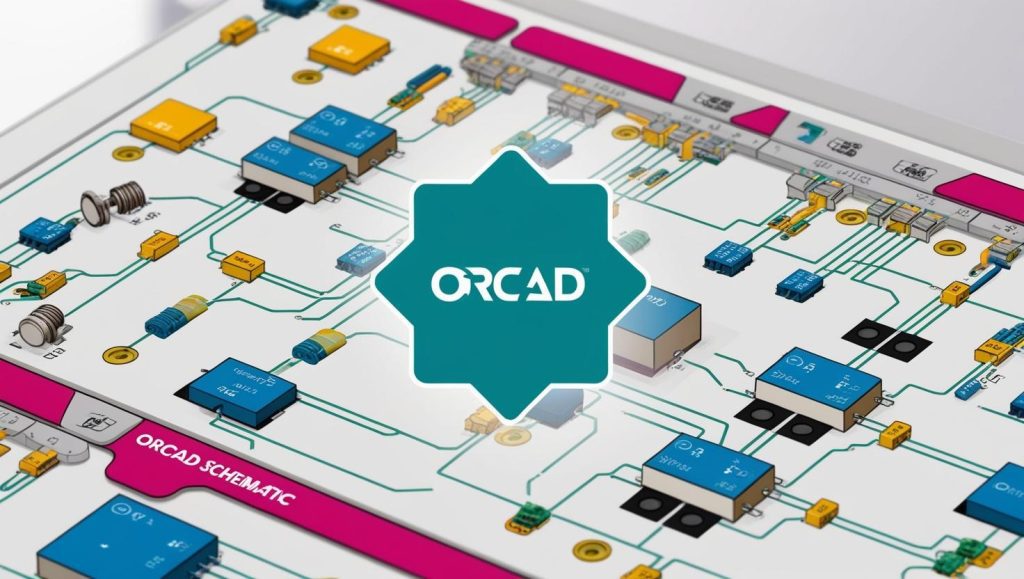
Key Features of OrCAD
- Schematic Capture: Allows users to create and edit circuit diagrams.
- PCB Design: Enables the creation of multilayer PCB layouts.
- Simulation & Analysis: Includes tools for SPICE-based circuit simulation.
- Library Management: Offers a vast component library for efficient design.
- Signal Integrity Analysis: Ensures the reliability of high-speed circuits.
For more details, visit Cadence OrCAD Official Page.
Applications of OrCAD in Engineering
1. PCB Design and Manufacturing
OrCAD simplifies PCB layout design, making it easy for engineers to transition from schematic capture to a final PCB layout.
2. Circuit Simulation and Analysis
Using OrCAD PSPICE, engineers can simulate circuits to analyze voltage, current, and power before physical implementation.
3. Signal Integrity and Power Analysis
OrCAD enables the evaluation of high-speed circuit behavior, ensuring minimal signal loss and noise.
4. Embedded System Design
OrCAD is used in the design and testing of embedded circuits for microcontrollers and FPGA-based applications.
For more insights, check IEEE Xplore for research papers on OrCAD applications.
Common Challenges in OrCAD Homework
1. Learning Curve for Beginners
New users often struggle with understanding OrCAD’s interface and tools.
2. Schematic Design Issues
Errors in schematic capture can lead to incorrect circuit behavior.
3. Simulation Errors
Incorrect component values or improper circuit connections can cause simulation failures.
4. PCB Layout Complexity
Placing components correctly and ensuring proper routing require practice.
To overcome these challenges, refer to OrCAD Tutorials.
Step-by-Step Guide to Solving OrCAD Assignments
Step 1: Understanding the Assignment Requirements
Identify the circuit to be designed and determine the necessary components and connections.
Step 2: Creating a Schematic in OrCAD Capture
- Open OrCAD Capture and create a new project.
- Select the appropriate components from the library.
- Connect the components using wiring tools.
Step 3: Running Circuit Simulation in PSPICE
- Set up a transient, AC, or DC analysis.
- Define input sources and load conditions.
- Run the simulation and analyze output waveforms.
Step 4: Designing the PCB Layout in OrCAD PCB Editor
- Convert the schematic into a PCB layout.
- Place components according to best practices.
- Route traces and check for design rule violations.
Step 5: Verifying and Optimizing the Design
- Perform a Design Rule Check (DRC).
- Optimize component placement and signal routing.
- Generate Gerber files for PCB manufacturing.
For hands-on training, check Coursera’s PCB Design Courses.
Best Online Resources for OrCAD Homework Help
- Cadence Learning Center – Official training materials.
- YouTube Channels like Robert Feranec – Practical tutorials.
- Stack Overflow – Community-driven problem-solving.
- ResearchGate – Academic papers on OrCAD applications.
Conclusion
Mastering OrCAD requires practice, patience, and a structured approach. This guide has outlined essential concepts, problem-solving strategies, and recommended resources for students seeking OrCAD Homework Help. Whether you’re struggling with schematic capture, simulation, or PCB design, using the right resources will make your learning journey smoother.
For the latest advancements in PCB design, visit Cadence OrCAD Blog.